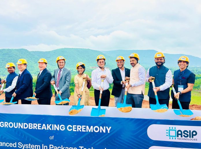
Prime Minister Mr Narendra Modi recently laid the foundation stone (virtually) and unveiled the plaque for ASIP Technologies semiconductor manufacturing facility at Tarluvada, Visakhapatnam.
The Rs 2,500 crore Outsourced Semiconductor Assembly and Test (OSAT) project is said to be Andhra Pradesh’s and South India’s first semiconductor manufacturing facility approved under the India Semiconductor Mission (ISM 1.0).
Andhra’s chief minister Mr N. Chandrababu Naidu joined the Prime Minister virtually for the foundation stone ceremony.
About ASIP
ASIP (Advanced System in Package Technologies) is a semiconductor packaging and testing company dedicated to establishing world-class Outsourced Semiconductor Assembly and Test (OSAT) capabilities in India.
Backed by global industry expertise, advanced manufacturing technologies, and strategic international partnerships, ASIP is building a state-of-the-art semiconductor packaging and testing facility to serve leading semiconductor companies across North America, Asia, and other global markets.
The company is committed to strengthening India’s role in the global semiconductor value chain through advanced packaging and testing solutions, talent development, technological innovation, and sustainable industrial growth.
South Korean Connection
The 30-acre facility, established with an initial investment of over Rs 460 crore in partnership with APACT Co., South Korea, as its technology partner, will have an annual production capacity of 96 million chips.
It will serve high-growth sectors, including artificial intelligence (AI), high-performance computing, data centres, and high-speed communications.
ASIP also plans to expand the facility with an additional investment of over Rs 2,000 crore to further scale up its advanced semiconductor packaging operations.
The project is expected to create over 1,000 direct high-skilled jobs and 1,600 indirect jobs.
Once operational, ASIP will commence production with wire-bond and Flip-Chip Ball Grid Array (BGA) packaging technologies, followed by the introduction of advanced 2.5D and 3D packaging capabilities within two to three years.
AP’s Workforce
Prime Minister Modi in his address commended Andhra Pradesh’s IT talent pool in software and now with the groundbreaking of semiconductor manufacturing facility it is well poised to lead in Semiconductor manufacturing sector, and the government is committed to back this emerging manufacturing growth story which is an important part of viksit bharat mission.
Mr. Amitesh Kumar Sinha, CEO, ISM, Govt. of India applauded ASIP breaking ground citing it as an important contribution and step forward to further India’s semiconductor mission, bringing advance semiconductor packaging facility in Visakhapatnam, Andhra Pradesh, he reaffirmed the ISM commitment to provide all the support through growth driven industry policies.
Mr. Venkata Simhadri, Managing Director and CEO of ASIP said “The groundbreaking of our Visakhapatnam facility marks a significant milestone for ASIP and our commitment to strengthening India’s semiconductor manufacturing capabilities.
Together with our partner APACT, we are establishing advanced assembly, packaging and testing capabilities in India, while driving skill development, supply chain localisation, and contributing to the growth of Andhra Pradesh’s semiconductor ecosystem.”
Similarly, Mr. Seong Dong Lee, CEO, President of APACT said: “The semiconductor industry is increasingly looking for resilient and diversified supply chains. Our partnership with ASIP combines Korean technology expertise with India’s engineering talent and manufacturing ambition.
We believe this facility will become an important part of India’s Semiconductor Mission and the global semiconductor ecosystem, providing advanced packaging and testing solutions to customers globally.”
India currently imports virtually all semiconductor chips used in its electronics industry.
This OSAT facility addresses a critical gap in the country’s semiconductor value chain, where packaging and testing account for roughly 30% to 40% of a chip’s manufacturing cost.
The company expects to localize a significant portion of its supply chain over the next three to five years while building partnerships with academic institutions, including IIT Tirupati and IIT Hyderabad.
The facility will also include an in-house semiconductor training center aimed at developing a skilled workforce for India’s growing semiconductor sector.
Sustainability features such as solar power generation and water recycling systems will be integrated into the project, with the goal of establishing a high-standard, environmentally responsible manufacturing operation.
Mr. Bhaskar Katamneni IAS, Secretary, IT, Electronics & Communication, Govt. of Andhra Pradesh, Mr. Mallavarapu Surya Teja, IAS Special Secretary, ITE&C Dept, Govt of Andhra Pradesh, were also present at the ceremony along with senior government officials, industry leaders and global partners.